Sourced from
docs/hardware/build-tft.mdin the firmware repo.
Build Guide - Touch TFT
How to construct the touch-screen Nimbus configuration from parts: a 2.8" ILI9341 240×320 color TFT with an XPT2046 resistive touch controller on the Solide S3 board (ESP32-S3-DevKitC-1 N16R8). The display and touch controller share the board's SPI3 pads, and the touch layer is the only input.
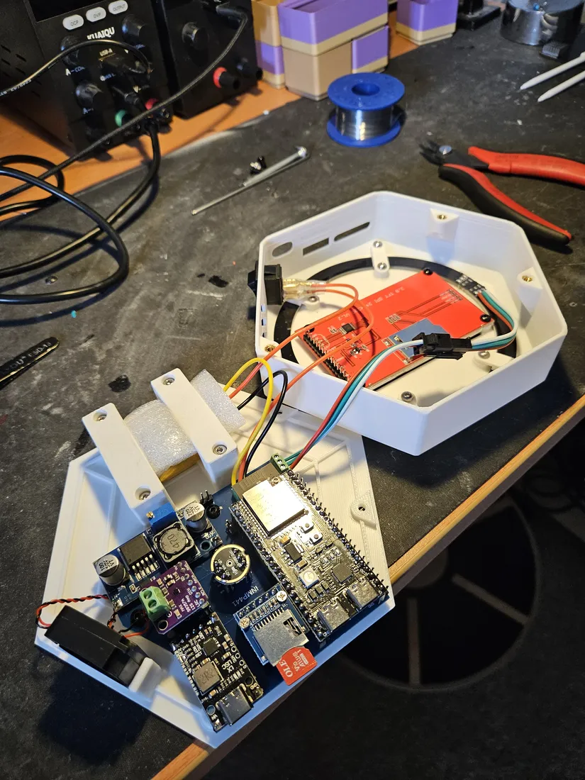
This page is the assembly walk-through. The companion pages:
- Touch TFT reference - the pinout drawing, touch calibration, screenshots, and the white-screen investigation.
- Hardware reference - everything common across the boards: first flash, shared peripherals, power, battery sensing.
Bill of materials
All commodity parts; any listing matching the Module / chip column works. Prices are approximate street prices in USD, excluding shipping. The consolidated parts list for all configurations, with the shared-parts breakdown and safety notes, is the bill of materials.
| Qty | Part | Module / chip | Notes | Purchase | ~Price |
|---|---|---|---|---|---|
| 1 | Dev board | ESP32-S3-DevKitC-1 N16R8 | 16 MB QIO flash, 8 MB octal PSRAM. The N16R8 variant specifically - octal PSRAM occupies GPIO 33–37. | AliExpress · Mouser | $12 |
| 1 | Display | 2.8" ILI9341 SPI TFT, 240×320, with XPT2046 resistive touch | The common SPI module with display pads (SCK/SDI/SDO/DC/RESET/CS/LED) plus a touch header (T_CLK/T_DIN/T_DO/T_CS/T_IRQ). Three on-module solder bridges are required - see below. | AliExpress | $8 |
| 1 | LED ring | WS2812B ring, 45 pixels | Addressable RGB; 5 V power, 3.3 V logic. | AliExpress | $6 |
| 1 | Amp | MAX98357A I²S amplifier breakout | Class-D, built-in thermal and over-current protection. | Adafruit 3006 · AliExpress | $2–6 |
| 1 | Speaker | 4 Ω · 3 W · ~40 mm full-range | The standard MAX98357A pairing; any small 4 Ω 3 W driver (28–45 mm) works. | AliExpress | $2 |
| 1 | Mic | INMP441 or ICS-43434 I²S MEMS mic breakout | Separate breakout from the amp. 3.3 V only - 5 V damages the S3. | AliExpress | $2 |
| 1 | Storage | microSD module (SPI) + microSD card | Card must be formatted FAT32 - see the trap below. | AliExpress + any 16–32 GB card | $6 |
| 2 | Cells | 18650 Li-ion | Wired in series (2S). Brand-name cells from a reputable vendor only. Reference pack: owner-measured 3500 mAh, 8.40 V full. | 18650batterystore.com | $12 |
| 1 | Charger/protection | 2S BMS with USB-C charging | Protection + balance + charging in one module. | AliExpress | $3 |
| 1 | Regulator | DC-DC converter → 5 V | From the 2S pack (~6.0–8.4 V) to a clean 5 V bus, ≥2 A. | AliExpress | $2 |
| 1 each | Battery sense | 220 kΩ + 100 kΩ resistors | Optional but recommended - the pack-voltage divider on GPIO 4. | any electronics supplier | $1 |
| - | Misc | wire, protoboard/PCB, JST connectors; optional 330 Ω resistor (LED DIN) and 1000 µF capacitor (ring 5 V/GND) | The resistor and capacitor improve LED reliability on long runs. | AliExpress | $5 |
Total: ≈ $59–63 (AliExpress-class sourcing; US distributors add ~$15–25).
The panel's touch layer is the only input.
Power architecture
- On battery: the DC-DC 5 V bus feeds the ESP32's VIN; the DevKit's on-board regulator makes the 3.3 V rail. USB-C on the BMS charges the pack.
- On USB alone (development): the DevKit runs from USB - the MCU, TFT, touch, SD, and mic all work. The LED ring will not light and the speaker will not drive audibly without the 5 V bus, which is the pack path.
- Every ground is common - tie all GNDs together: cells, BMS, DC-DC, ESP32, and every module.
- ⚠ The mic VCC is 3.3 V only. Its VDD and data lines follow VCC, and 5 V damages the S3's input. Never put the mic on the 5 V bus.
- ⚠ The TFT backlight is a continuous draw whenever it is lit. It sits on a PWM pin so the firmware's idle path blanks it rather than drawing a screensaver.
The three on-module solder bridges (do this first)
The XPT2046 touch header is not wired to three additional ESP32 GPIOs. Before wiring the module to the board, solder three short jumpers on the TFT module itself so touch and display share one SPI bus:
| Touch pad | Jumper to display pad | Shared ESP32 net |
|---|---|---|
T_CLK | SCK | GPIO 42 - SPI clock |
T_DIN | SDI | GPIO 41 - SPI MOSI |
T_DO | SDO | GPIO 1 - SPI MISO |
These are physical pad-to-pad connections on the module, not three more wires
to the DevKit. Connect T_CS separately to GPIO 48. Leave T_IRQ
unconnected; Nimbus polls the touch controller.
⚠ Continuity-check all three pairs with power disconnected. The ESP32 bus
wire may land on either pad of a pair, but both pads must be electrically
common. Missing bridges can leave the display completely blank (bus wires on
the touch-side pads) or leave the display working while touch is dead (bus
wires on the display-side pads). Also verify T_CS → GPIO 48 and confirm
T_IRQ has not accidentally been connected to GPIO 48.
Wiring
The whole build at block level - each peripheral with its bus and rail, and the battery chain along the bottom (the pin-by-pin tables follow):

Copied from the Touch TFT reference - the display and touch table first, then the shared peripherals from the solide-drivers build guide.
TFT + touch (SPI3)
| ESP32 GPIO | Net | Module pins |
|---|---|---|
| 42 | SPI clock | SCK + T_CLK |
| 41 | SPI MOSI | SDI + T_DIN |
| 1 | SPI MISO | SDO + T_DO |
| 40 | display D/C | DC |
| 39 | display reset | RESET |
| 38 | display CS | CS |
| 48 | touch CS | T_CS |
| 2 | backlight (PWM) | LED |
| - | not connected | T_IRQ |
| 3V3 / GND | power | VCC / GND |
The three on-module bridges make display and touch one SPI bus with two chip selects, which is what fits the whole panel into seven GPIOs.
microSD module (SPI2 - a separate bus)
| Module pin | → | ESP32 |
|---|---|---|
| VCC (3V3) | → | 3V3 |
| GND | → | GND |
| CS | → | GPIO 10 |
| MOSI (DI) | → | GPIO 11 |
| SCK (CLK) | → | GPIO 12 |
| MISO (DO) | → | GPIO 13 |
The SD is not on the TFT's SPI bus - they share only 3.3 V and ground.
WS2812B LED ring
| Module pin | → | ESP32 / rail |
|---|---|---|
| +5V | → | 5 V bus |
| GND | → | GND (common) |
| DIN | → | GPIO 21 (a 330 Ω series resistor on DIN is good practice) |
Audio - MAX98357A amp + I²S mic
Two separate breakouts. The amp runs at reduced volume on 3.3 V (fine as a status speaker); use the 5 V bus for more volume - but never share that VCC with the mic.
| Module | Pin | Role | → | ESP32 / rail |
|---|---|---|---|---|
| amp | VCC | power | → | 3V3 (5 V bus for louder) |
| amp | GND | ground | → | GND |
| amp | BCLK | bit clock | → | GPIO 7 |
| amp | LRCLK | word clock | → | GPIO 8 |
| amp | DIN | data in | → | GPIO 17 |
| mic | VDD | power | → | 3V3 ⚠ (never 5 V) |
| mic | GND | ground | → | GND |
| mic | BCLK / SCK | bit clock | → | GPIO 15 |
| mic | WS / LRCLK | word select | → | GPIO 18 |
| mic | SD | data out | → | GPIO 16 |
| mic | L/R | channel select | → | GND (left slot) |
Battery sense (optional, recommended)
A 220 kΩ / 100 kΩ divider from the pack (before the DC-DC) into GPIO 4 (ADC1). See Battery voltage sampling.
Assembly walk-through
A photo-by-photo build of an actual Nimbus, from printed parts to the finished device. The wiring tables above are the pin-level authority; this section is the physical order of operations. On this build the three on-module solder bridges come first, before any step below. Bench-flash and self-test each subsystem (the Assembly order below) before you close the case.
Print the case and set the heat inserts
Print all enclosure parts before you touch the electronics. STL, material, and support notes live in Enclosure and CAD - print in PLA or PETG, main body needs no supports on most printers.
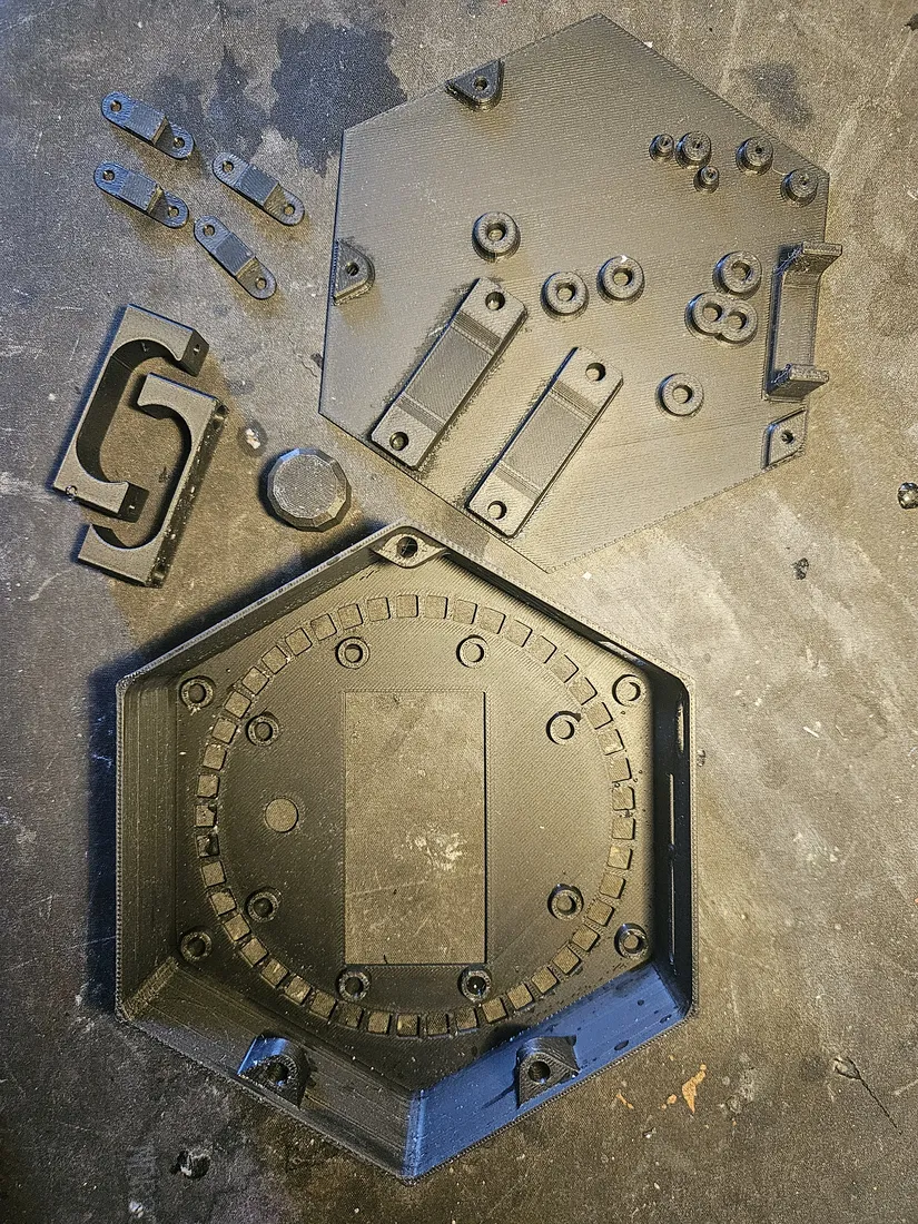
Confirm the print set is complete. Lay every part out and account for it before starting. This build uses:
- the top plate (upper right) - flat hexagon carrying the board standoffs, two long rail mounts, and the clustered mounting bosses;
- the bottom tub (lower) - deep hexagon with the circular LED-ring channel and the rectangular center pocket;
- the small clip brackets and the S-logo bracket (left);
- the hex plug (center left).
Check that the boss holes printed clean and open. If a hole bridged over or is stringy, clear it before pressing an insert - an insert will not seat square in a fouled hole.
Set the inserts in the tub half. Press a brass heat-set insert into each boss around the LED-ring channel and into the corner posts.
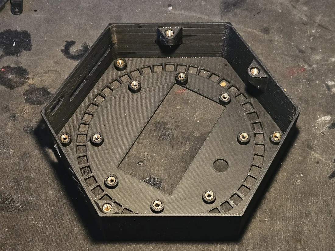
Use a soldering iron fitted with an insert tip (or a plain conical tip). Follow the iron's own guidance for temperature and the insert maker's recommended setting - do not guess a number. Rest the insert on the hole, let it heat, then press straight down so the knurled body sinks into the plastic. Check each one: the insert should sit flush or a hair below the boss face, square to the surface, with a small bead of melted plastic pushed up around it. Wipe stray plastic off the threads while it is still warm.
Set the inserts in the plate half. Repeat for every boss on the top plate, including the two long rail mounts and the standoff clusters.
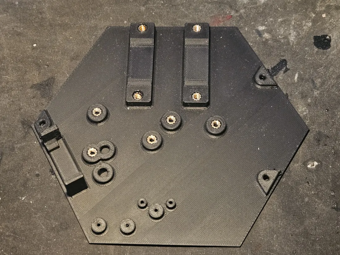
The plate carries more inserts and they sit at different heights on the raised standoffs. Keep each one vertical as it sinks - a leaning insert throws off board alignment later. Confirm the two inserts at the ends of each rail mount are flush; those take the load when the assembly is screwed together. Let the whole part cool fully before you thread anything into a fresh insert.
Fastener note: the microSD holder screws. The microSD holder module stands taller than the flat-seated parts, so it uses a longer pair of screws than the rest of the assembly.
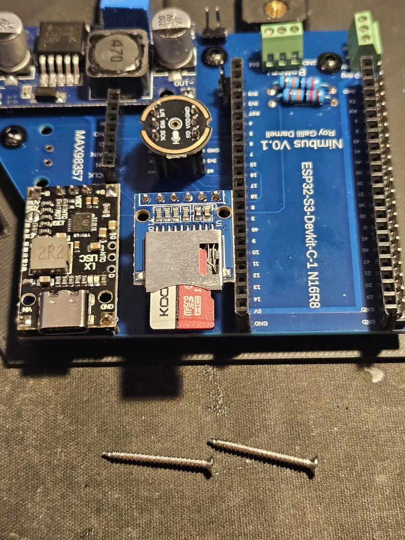
Set the two longer screws (shown on the bench beneath the board) aside with the SD holder so they do not get mixed into the shorter case hardware. Match screw length to what each part actually needs - a screw too long will bottom out or push past a boss. If you are unsure of a length, match it against the part before driving it.
Seat inserts and dry-fit the case, but leave the board and Li-ion pack out until wiring is done. Keep the earlier safety framing in view once electronics go in: brand-name cells only, the 2S BMS stays between the cells and everything else, never charge the pack outside the BMS, verify a clean 5V at the DC-DC output with a meter before the board or pack is connected, tie every ground common, and treat any warm or hot module or SD card as an electrical fault - power off first. The firmware caps LED brightness at 60% and it must not be raised.
Assemble the carrier board
There are two ways to wire a Nimbus. This section covers the optional custom carrier PCB (Nimbus V0.1) - a single blue board that sockets the DevKit and every module and routes the power section for you. If you would rather hand-wire, skip this section entirely and build on protoboard straight from the Wiring tables - the carrier PCB carries no signals the tables do not, it just makes them solder-free. The manufacturing outputs (Gerbers, ODB++, CAM) to order your own board live in hardware/fab/; see how to order the board.
The whole point of the board is that nothing is soldered down permanently. The DevKit and the small modules drop into female headers, so any one of them can be pulled and replaced. Solder the headers, not the modules.
The DevKit
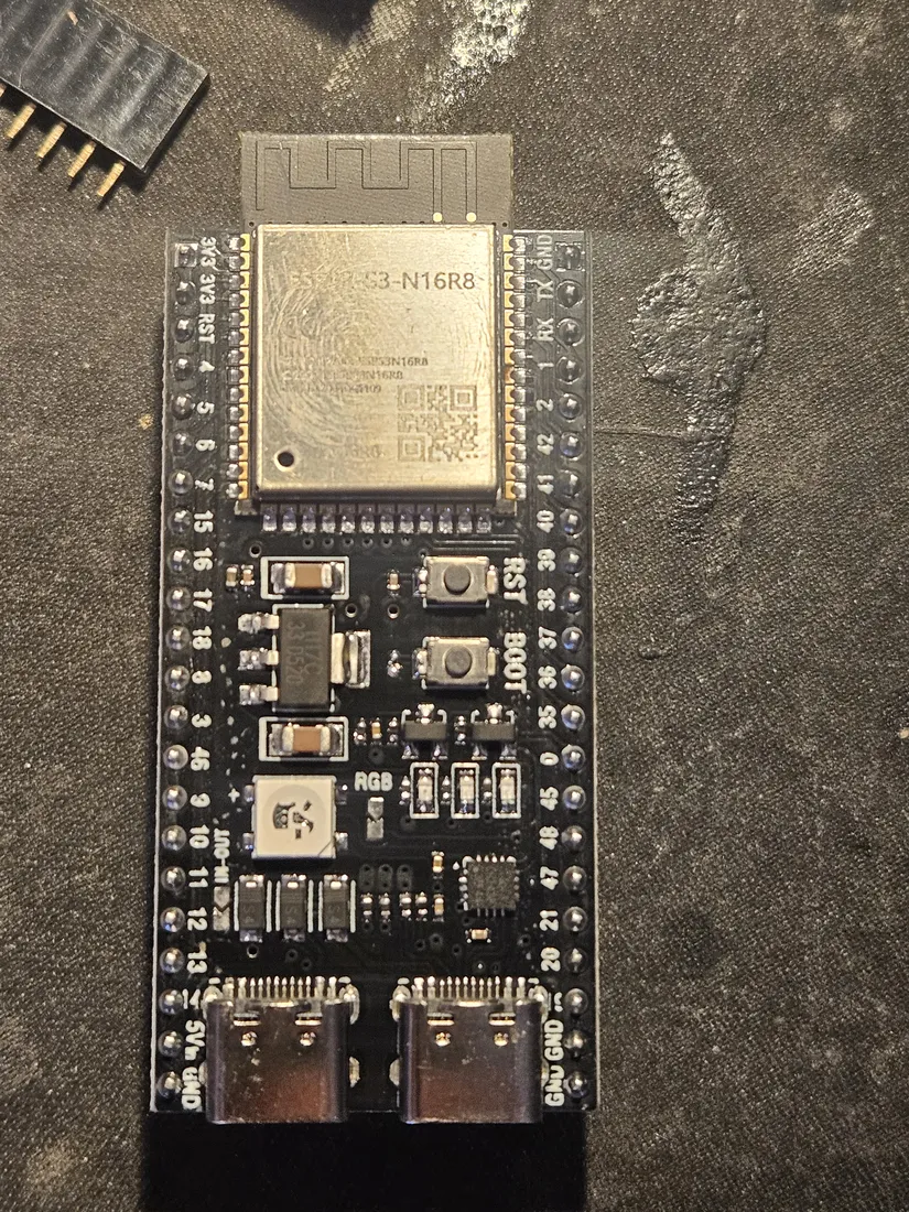
The brain is the ESP32-S3-DevKitC-1 N16R8 - the wide black board with the shielded ESP32-S3-N16R8 module and two USB-C ports at the bottom edge. The two ports are not interchangeable: one is the UART bridge and one is the native USB. Flash a fresh board over the UART port - see First flash of a fresh board - before you commit it to the carrier. The pin numbers silkscreened down both long edges (3V3, RST, 4, 5, 6 ... on one side; GND, TX, RX, 1, 2, 42 ... on the other) are the same numbers the Wiring tables use. Note the loose black header strip in the corner of the photo: that is the part you solder to the carrier, not to the DevKit.
The modules
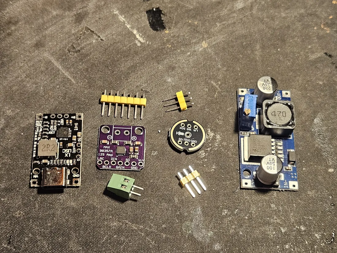
Everything that sockets into the carrier, laid out. From the parts in the bill of materials: the purple MAX98357A I²S amp (with its green 2-position speaker screw terminal), the round INMP441 I²S mic breakout, the blue DC-DC LM2596 buck converter (the large module with the 470 inductor, the 100/220 electrolytics, and the blue trimmer pot), and the black USB-C charger/BMS board. Also shown are the male header strips for the module breakouts. Keep the mic separate in your mind from the amp - they are two different breakouts, and the mic is 3.3 V only.
The bare board, top
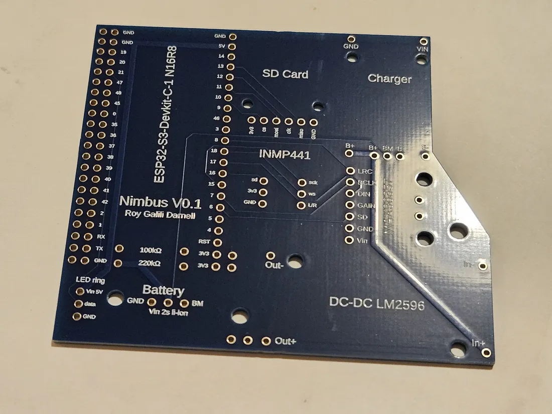
The bare carrier, top side. Read the silkscreen before you solder anything - every footprint is named:
- ESP32-S3-Devkit-C-1 N16R8 - the two long through-hole rows down the left that the DevKit straddles.
- SD Card, INMP441, MAX98357 - the three module rows across the middle, each with its pin names (
cs/mosi/clk/miso,sck/ws/sd/L/R,LRC/BCLK/DIN/GAIN/SD/Vin). - Charger and DC-DC LM2596 - the power section on the right, with the
B+/BM/B-,VIN, andIn+/In-/Out+/Out-pads. - Battery (
GND/Vin 2s li-ion/BM) and LED ring (Vin 5V/data/GND) at the bottom left, plus the 100kΩ / 220kΩ footprint for the battery-sense divider.
Every pad name maps one-to-one to a row in the Wiring tables. When in doubt, the silk is the authority.
The bare board, back
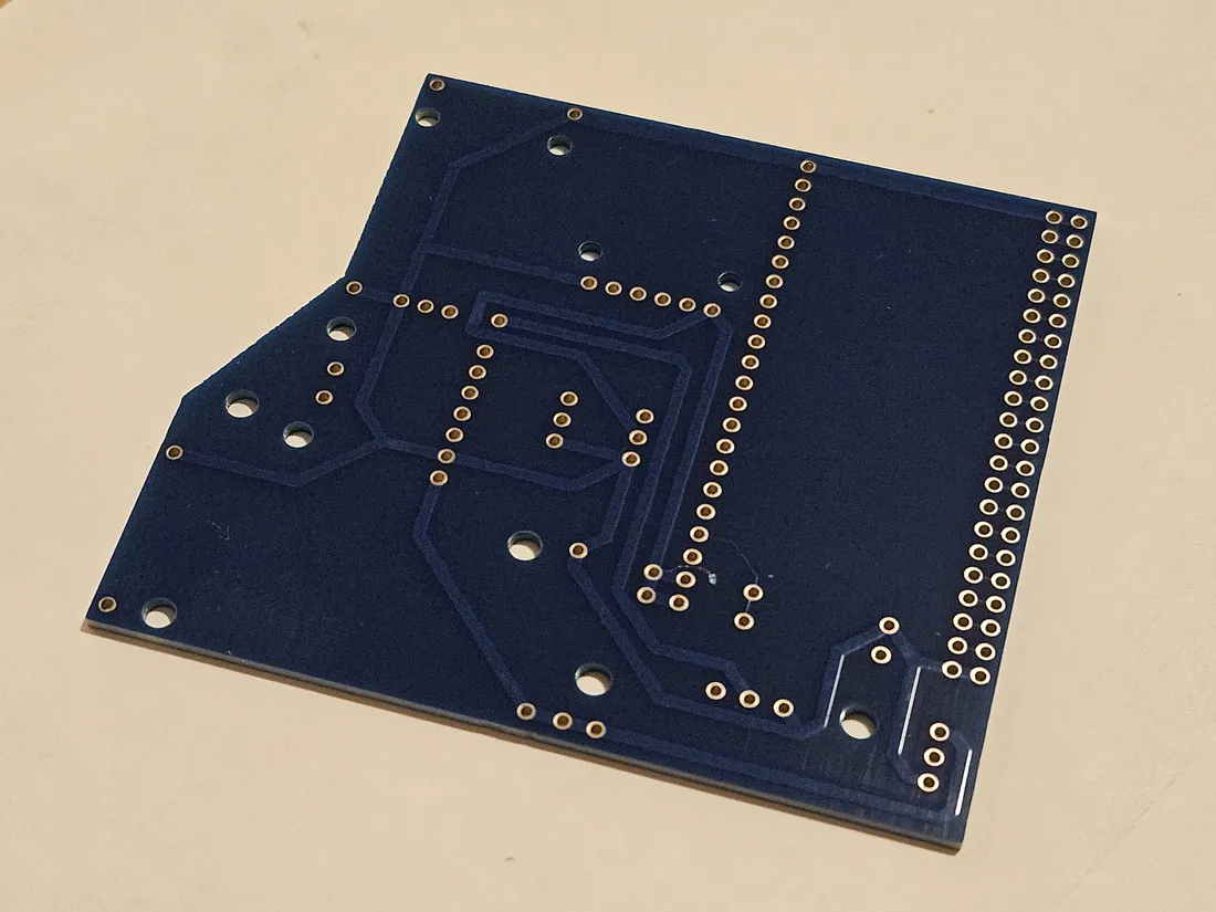
The back, bare. This is where all your solder joints will land, so give it a look first: the plated through-holes and the routed traces should be clean and unbridged out of the box. Nothing mounts on this side - components all sit on the top.
The routing, for reference
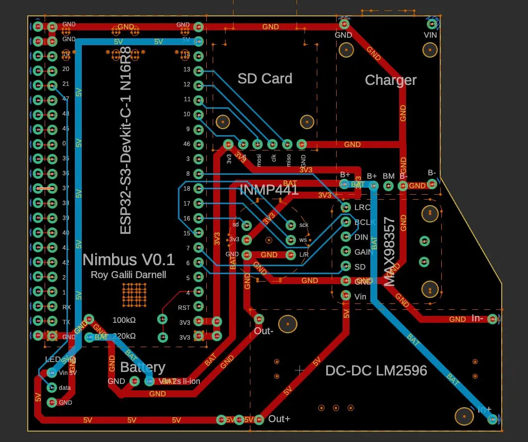
Not a build step - the board layout, for anyone who wants to trace a net or fork the design. It shows how the four nets (raw BAT from the pack, the regulated 5V bus, 3V3, and a common GND) reach every module. It is the visual companion to Power architecture: the pack feeds the DC-DC, the DC-DC feeds the 5 V bus, the DevKit's on-board regulator makes 3.3 V, and every ground is tied common.
Solder the female headers
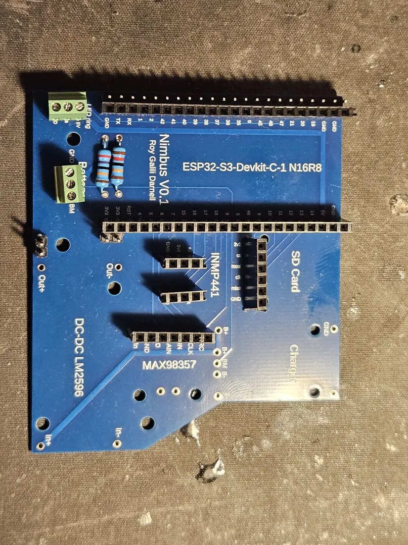
Set the headers. Cut female header strips to the length of each row and solder them in from the top so the sockets face up: the two long rows for the DevKit, and one short row each for the SD Card, INMP441, and MAX98357 footprints. Tack one end pin, check the strip sits flat and square against the board, then solder the rest. Straight headers here are what let you unplug a module later.
Set the fixed parts. While the iron is hot, place the two battery-sense resistors in the 100kΩ / 220kΩ footprint (the divider into GPIO 4 - see Battery sense), and the green screw terminals at the Battery and LED ring positions. These few parts do solder down; the modules do not. Check the finished joints are shiny and full, with none bridged to a neighbor.
Seat the charger and DC-DC
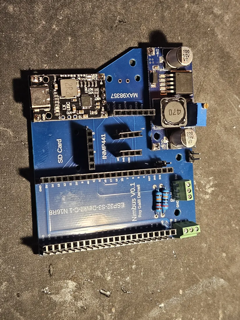
Mount the two large power modules at their labeled edge footprints: the DC-DC LM2596 at the In+/In-/Out+/Out- pads and the charger/BMS at the Charger pads (B+/BM/B-, VIN). Their outputs are the 5 V bus and the pack rail, so get the polarity right against the silk.
Li-ion safety is not optional here. Buy brand-name cells from a reputable vendor - counterfeits are common. The 2S BMS stays between the cells and everything else - the pack wires land on the charger/BMS, never straight onto the DC-DC or a module. Never charge the pack outside the BMS. Set the DC-DC output before you connect the DevKit: with the pack on the charger, turn the blue trimmer until a meter reads a clean 5 V at Out+/Out-, as called out in Power architecture.
Seat the DevKit and modules
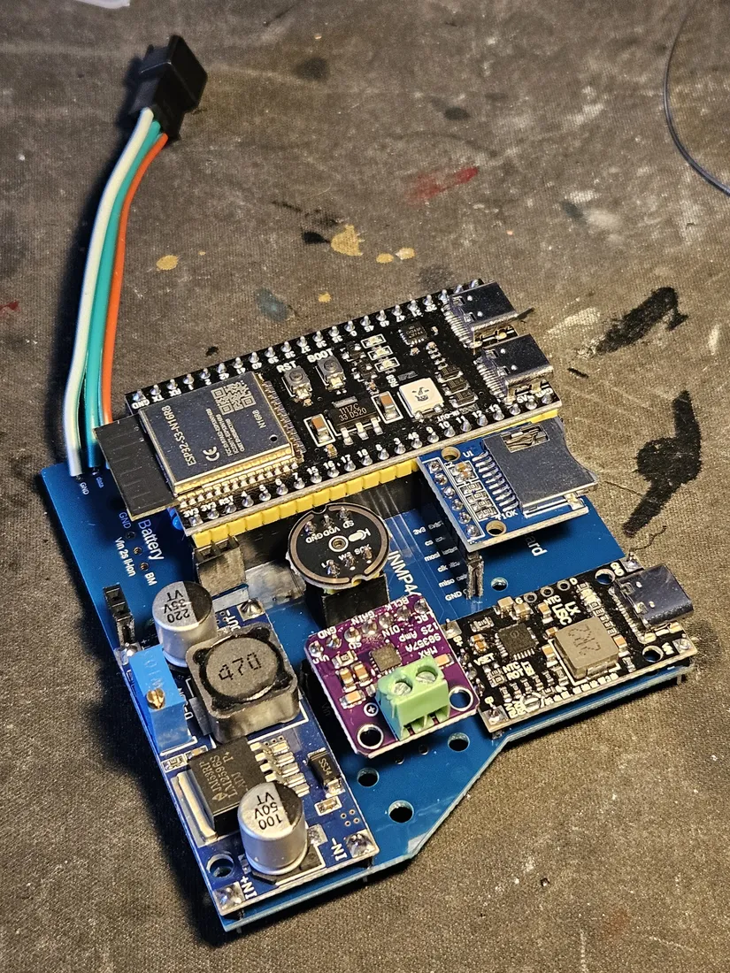
Seat the board. Push the DevKit into its two header rows so both USB-C ports overhang the board edge and stay reachable, and so its silk pin numbers line up with the carrier's. Then drop in the three small modules - SD card, INMP441 mic, MAX98357 amp - matching each module's pin labels to the socket labels beneath it. The amp's green screw terminal is the speaker output.
Connect the pack. The three-conductor lead at the top left is the 2S pack: it lands on the Battery input (GND, Vin 2s li-ion, BM) - pack negative, the balance mid-tap, and pack positive - which routes to the BMS, not to anything downstream. Confirm every ground is common before power-on.
The firmware caps LED-ring brightness at 60% for thermal safety; do not raise that limit. And once running, treat any warm module or a warm SD card as an electrical fault - power off first, then debug (see the hot-card safety check).
Check the back
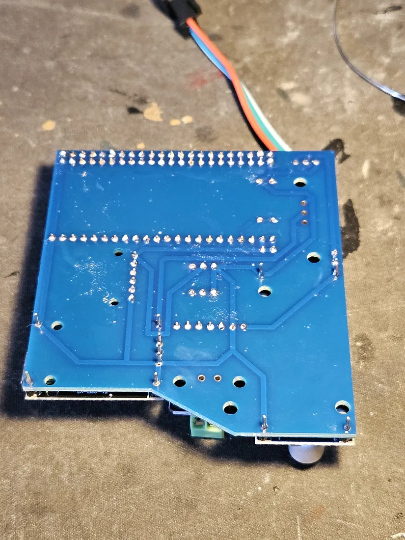
Flip it and inspect. Every header row should show a clean line of full, shiny joints with no cold joints and no bridges between adjacent pins - the DevKit rows and the module rows are the ones to scrutinize, since a single bridge there can short a rail into a signal. With the joints good and the pack on the BMS, the board is ready for the Wiring verification and first flash.
LED ring, speaker, and power switch
Three ring-and-shell parts finish the build: the WS2812B light ring behind the face, the status speaker in its pocket, and the rocker that switches pack power. Wire them per the pinout tables already in this page - do not re-derive the pins here.
1. Identify the ring and its pigtail.
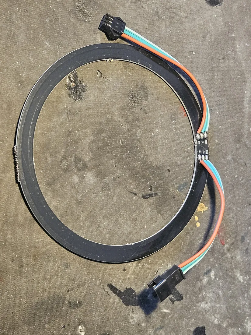
The ring is a flexible 45-pixel WS2812B on a black PCB. A three-conductor pigtail is soldered to the three pads at one point on the ring and runs out to a 3-pin JST connector: one conductor for +5V, one for GND, one for DIN. Confirm which pad is which against the silkscreen before you trust the wire colors - the colors are just whatever the pigtail shipped with and carry no standard meaning. Land those three wires exactly as the WS2812B LED ring table specifies: +5V to the 5 V bus, GND common, DIN to the data pin (a 330 Ω series resistor on DIN is good practice). Power the +5V leg only from the 5 V bus, never from 3V3.
2. Cut the ring open for the case pass-through.
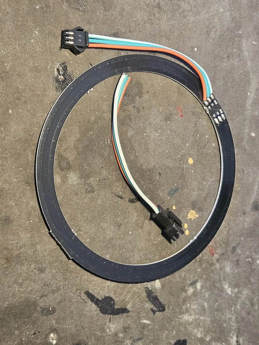
The ring must open at one spot so the pigtail can drop straight through the case wall instead of being pinched around the rim. Cut the single power ribbon that bridges the ring's two ends closed, at the seam next to where the pigtail attaches. Cut that ribbon only - never cut the LED strip itself, and do not nick or sever the three pigtail conductors; they must stay intact and carry the signal. The pixels are a single addressable chain, so any break in the strip kills every pixel downstream of it - the power ribbon is the one and only thing you cut. Route the pigtail through the case opening and reseat the ring so the open ends sit flush.
Brightness cap. The firmware caps the ring at 60% brightness and this cap must not be raised. It is a thermal and current limit for a 45-pixel ring on this pack, not a preference. Leave it where it is.
3. Prep the speaker.
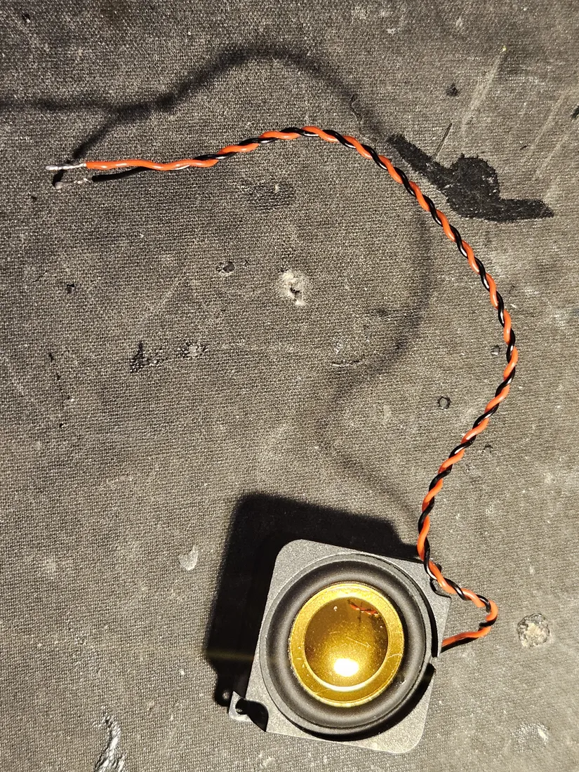
The speaker is the small 4 Ω full-range driver in a square frame. It comes with a twisted red/black lead pair, tinned at the free ends. This is a bare driver with no polarity that matters for a mono status tone, but keep the pair twisted to hold noise down. Land the two leads on the amp's speaker output per the Audio wiring section - the driver connects to the MAX98357A output, not to any ESP32 pin or rail directly.
4. Mount the speaker in the case.
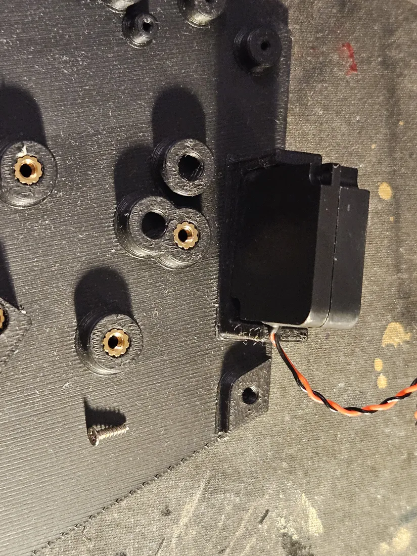
Seat the driver into its printed pocket so the frame sits flat against the shelf and the cone faces the grille. Fix it with the frame's mounting tab against the printed post; drive the self-tapping screw shown into the post - use the screw that fits the printed boss, do not overtighten into the plastic. Route the twisted lead pair out through the channel toward the amp. Check that the frame is fully seated and the cone is not fouling any wall before you close up. A speaker enclosure that buzzes is almost always a loose frame or a lead trapped under the cone, not a bad driver.
5. Press in the power rocker.
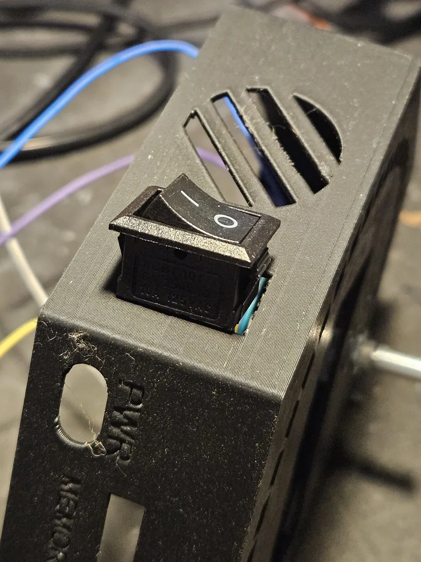
The rocker drops into the rectangular cutout in the case top, beside the vent slots and above the embossed PWR marking. Wire it before you press it home: the switch breaks the pack power line, so its two spade terminals go inline on the main power feed, one lead in and one out. Push the switch straight into the cutout until both retaining clips snap and the bezel sits flush with the case face. It should hold with no adhesive. The I / O markings on the paddle are the live/off states; confirm the paddle throws freely once seated and that the leads clear the vent slots.
This switch sits ahead of everything downstream but the pack always stays behind its 2S BMS - never bypass the BMS to reach the cells, and never charge the pack outside it. Keep every ground common across the ring, speaker, and switch. If any module or the SD card runs warm or hot, that is an electrical fault: throw the rocker to off first, then investigate.
Build the 2S battery pack
Read this before you touch a cell - 2S Li-ion. Two 18650s in series hold real energy, and this is the one stage of the build that can burn you or start a fire. Buy brand-name cells from a reputable vendor (the reference pack uses matched LiitoKala Lii-35A); counterfeit 18650s are common and dangerous. The 2S BMS stays between the cells and everything else - it is the only protection, balance, and charge path, so never charge the pack outside the BMS and never feed the DC-DC from anything but the BMS output. Tie every ground common. If a cell, a module, or the SD card ever gets warm that should not, treat it as an electrical fault: power off first, debug second. Work on one joint at a time, keep the two pack leads from ever touching, and never leave a bare cell terminal exposed. Full framing lives in the 2S Li-ion safety note and Power architecture.
Build the pack as its own sub-assembly and verify a clean 5 V at the DC-DC output before it feeds anything downstream. This is step 4 of the Assembly order; do not connect the 5 V bus to VIN or the LED ring until the meter reads right.
1. Insulate the cell tops.
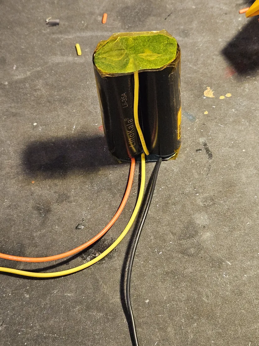
Lay the two cells side by side, same polarity conventions as your series plan, and cap the terminal ends with an insulating barrier before any metal goes near them. Here a sheet of fish-paper (Kapton works too) is taped down over the top of the pack so only the intended weld points are exposed. Check that the wraps on both cells are intact with no nicks down to bare steel, and that the insulator sits flat with no bare terminal ring peeking out from under the tape. The pack leads exit the opposite end.
2. Spot-weld the series link.
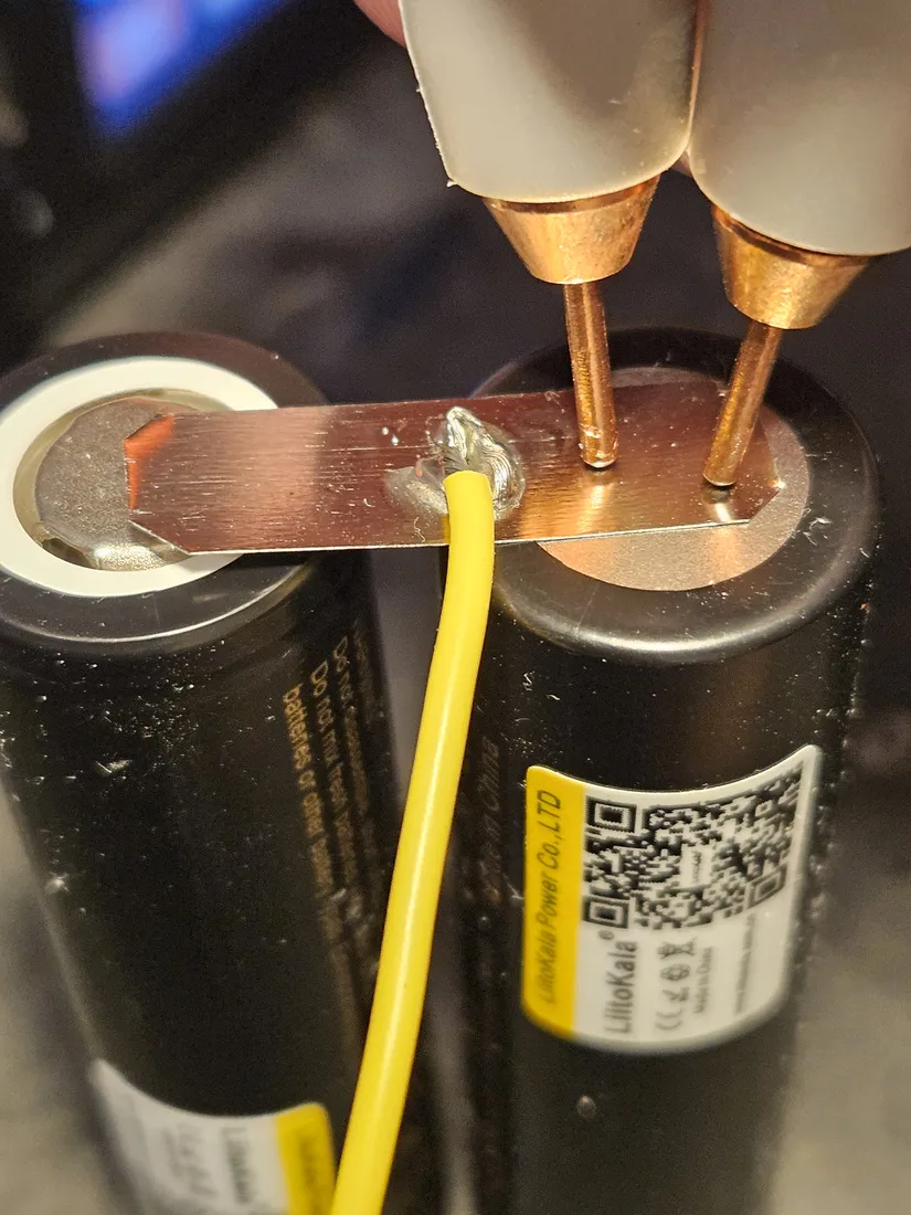
Bridge the two cells with a nickel strip and spot-weld it down - this is the series (2S) link that turns two cells into one 6.0–8.4 V pack. Both copper electrodes must land on the strip over the cell can, never bridging directly cell-to-cell. Do not solder this joint and do not guess the weld setting: dial the welder in on a scrap strip and cell first, per the welder's own guidance, until you get welds that bite without blowing through. Check each joint by tugging the strip lightly - it should not peel - and confirm you see clean weld dimples, not a scorched or lifted strip.
3. Solder the BMS pack lead.
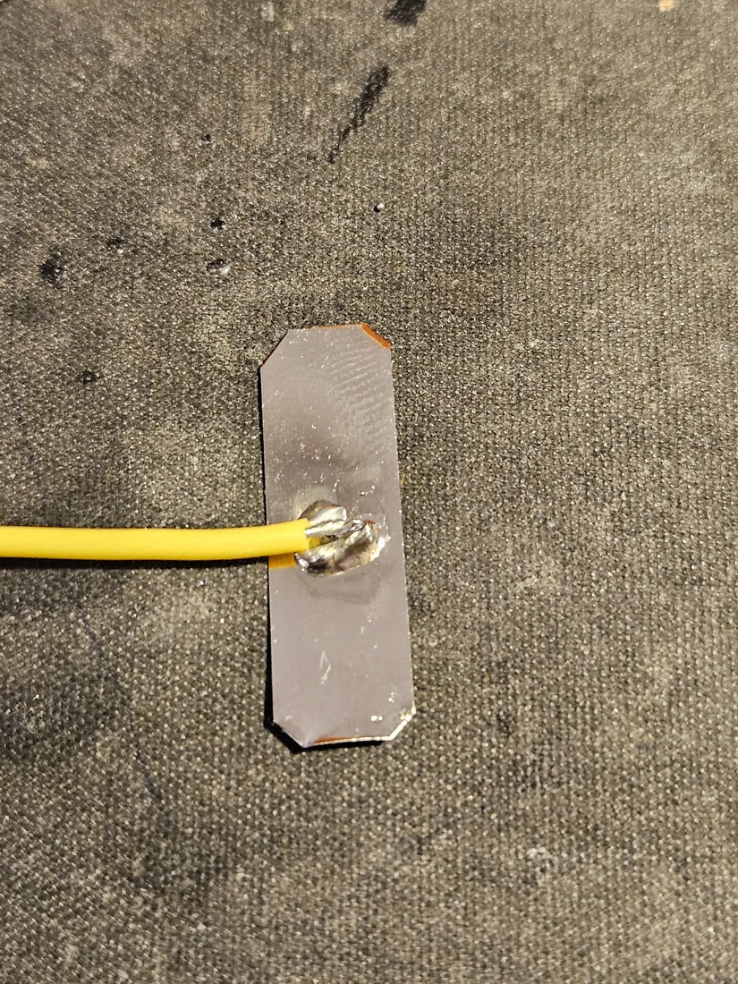
Solder the pack lead to its nickel tab as shown, keeping the iron on the tab and off the cell body. Use a hot, tinned iron and get in and out fast - follow your iron's guidance rather than any fixed temperature, because prolonged heat into an 18650 is what damages it. A good joint is a shiny, concave fillet with the wire fully anchored, not a dull gray blob. Let it cool before flexing.
4. Confirm the mid-point tap sits between the cells.
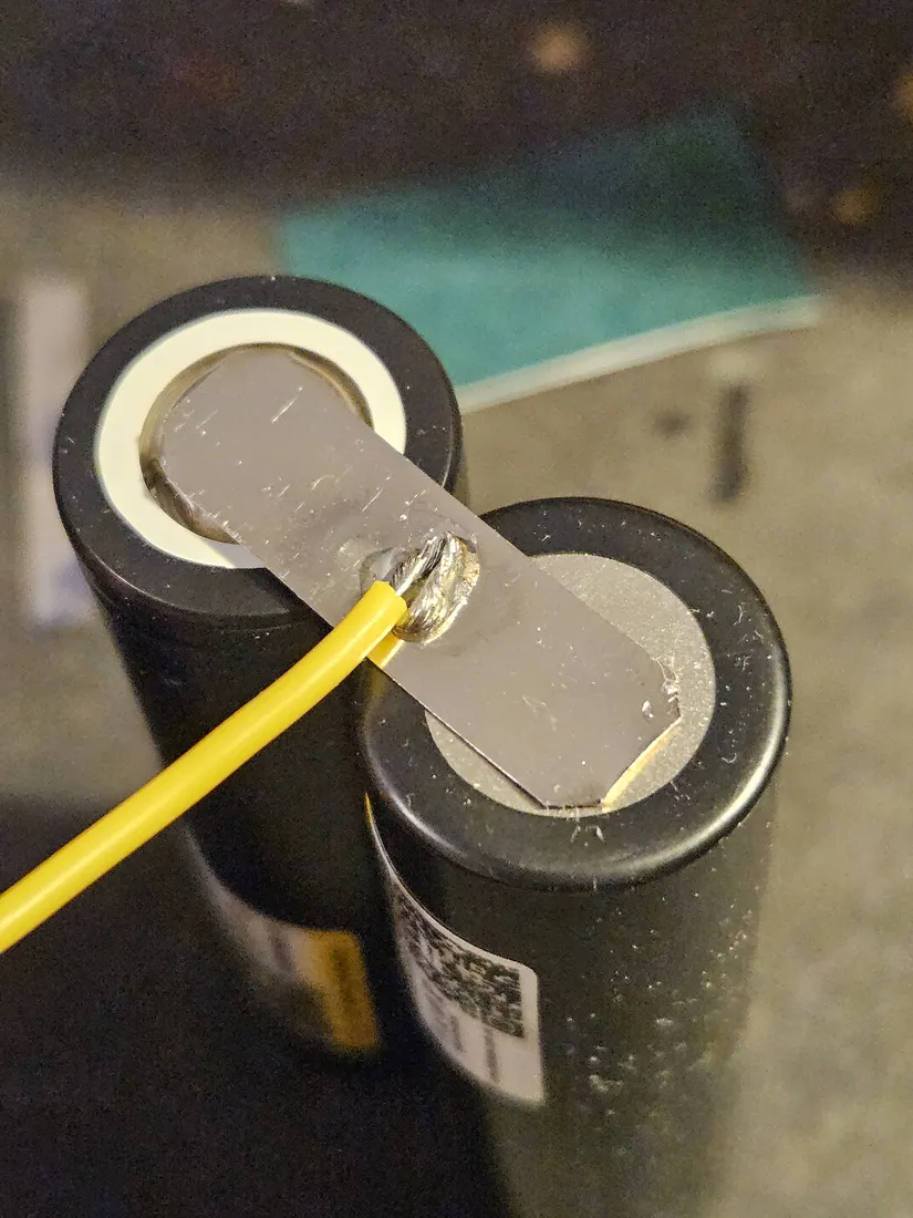
The strip now joins the two cell terminals and the tap wire lands at that series junction. This mid-point is the balance/sense tap that goes to the BMS, which is what places the BMS electrically between the cells so it can watch each one independently. Route this tap and the two pack leads to the BMS, never straight to the DC-DC. Verify the junction is solid and the tap wire is not shorting to the adjacent cell can. If your BMS labels its tap pads differently, follow its silk screen and datasheet for which lead is the mid-point.
5. Terminate the pack lead.
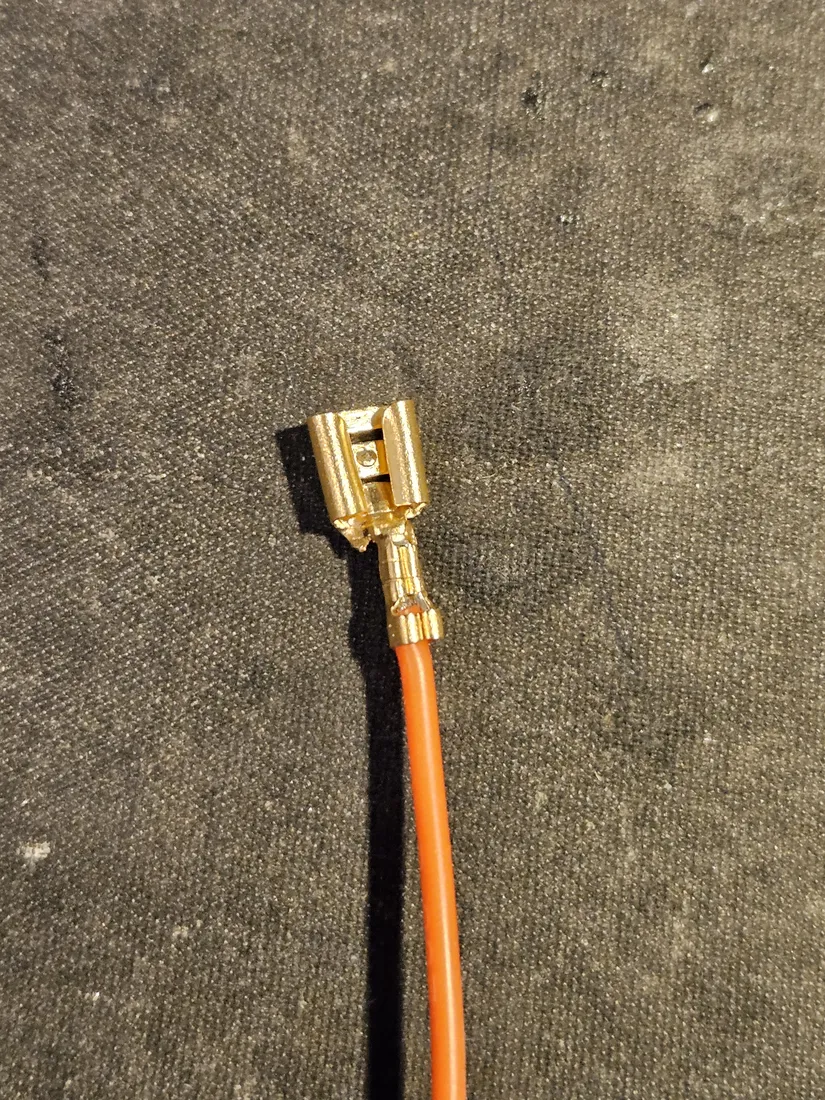
Crimp a female spade terminal onto the pack output lead so it lands on the board without a bare soldered wire flapping loose. Use the correct crimp for the wire (do not eyeball the terminal size) and crimp both the conductor barrel and the insulation grip. Check that the terminal grips copper, not just insulation, that no whiskers stick out, and give it a firm pull - it must not slide off. A heat-shrink collar over the crimp keeps it from shorting to a neighbour.
6. Connect the pack to the board.
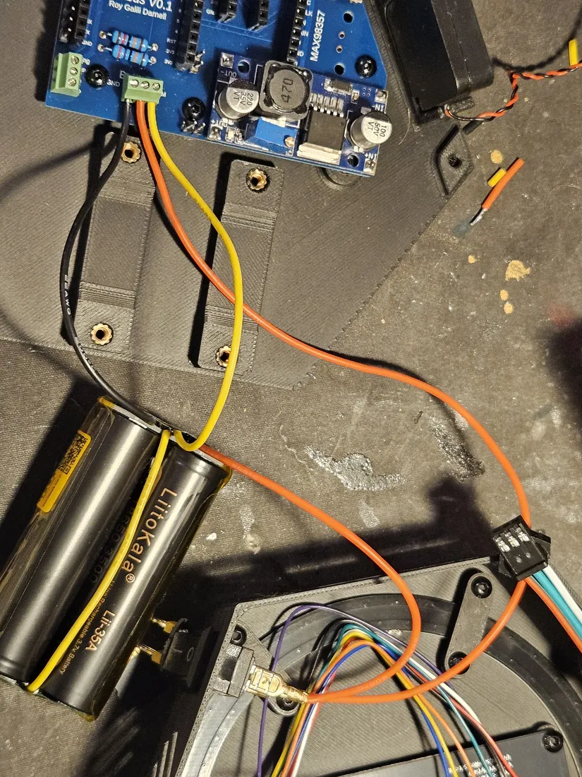
Land the pack leads on the board so the BMS output feeds the DC-DC input only at this point. Get polarity right before anything is energized - a reversed pack is how boards die. Confirm every ground is common between cells, BMS, DC-DC, and the board per Power architecture. Leave the 5 V bus disconnected from the ESP32 VIN and the LED ring until the next step passes; a mis-set converter must not be allowed to reach the MCU or the ring.
7. Calibrate the DC-DC to a clean 5 V, then stop.
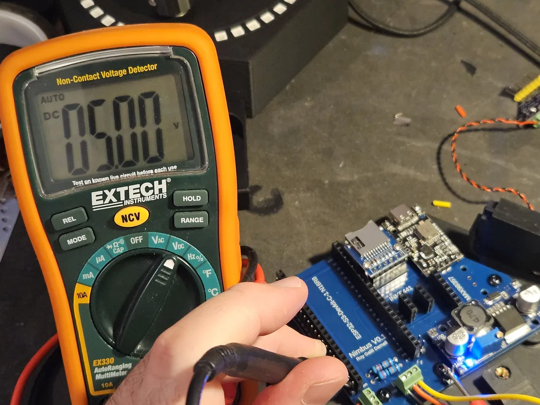
With the pack feeding the DC-DC input and nothing on the output yet, set the meter to DC volts and read across the converter's OUT + and OUT -. Turn the module's trim pot until it reads a clean 5.00 V, exactly as the meter shows here. This gate is non-negotiable: a converter shipped at 8 V or wandering under load will destroy the ESP32 and the ring the instant they are connected. Only once you have a steady 5.00 V do you wire the 5 V bus to VIN and the LED ring +5 V (step 5 of the Assembly order).
After the pack is assembled and running, charge it fully through the BMS USB-C port and run BATTCAL on the console so the gauge reads 100 % at full - the ADC under-reads a full pack. See Battery pack and Battery voltage sampling. Remember the firmware caps LED brightness at 60 %: sustained higher levels can overheat and damage the internal electronics, and must not be raised.
Stack the electronics and close the case
Do the full electrical bring-up before anything goes into the case. Once the boards are stacked and screwed down, the pin headers and the self-test console are hard to reach - so flash and pass the self-test on the bench first, following Assembly order steps 1-5: first flash over the UART port (First flash of a fresh board), then TEST all on the self-test console with led/screen/sd/memory/input all PASS. A board that boots clean loose on the bench is the only board worth closing up.
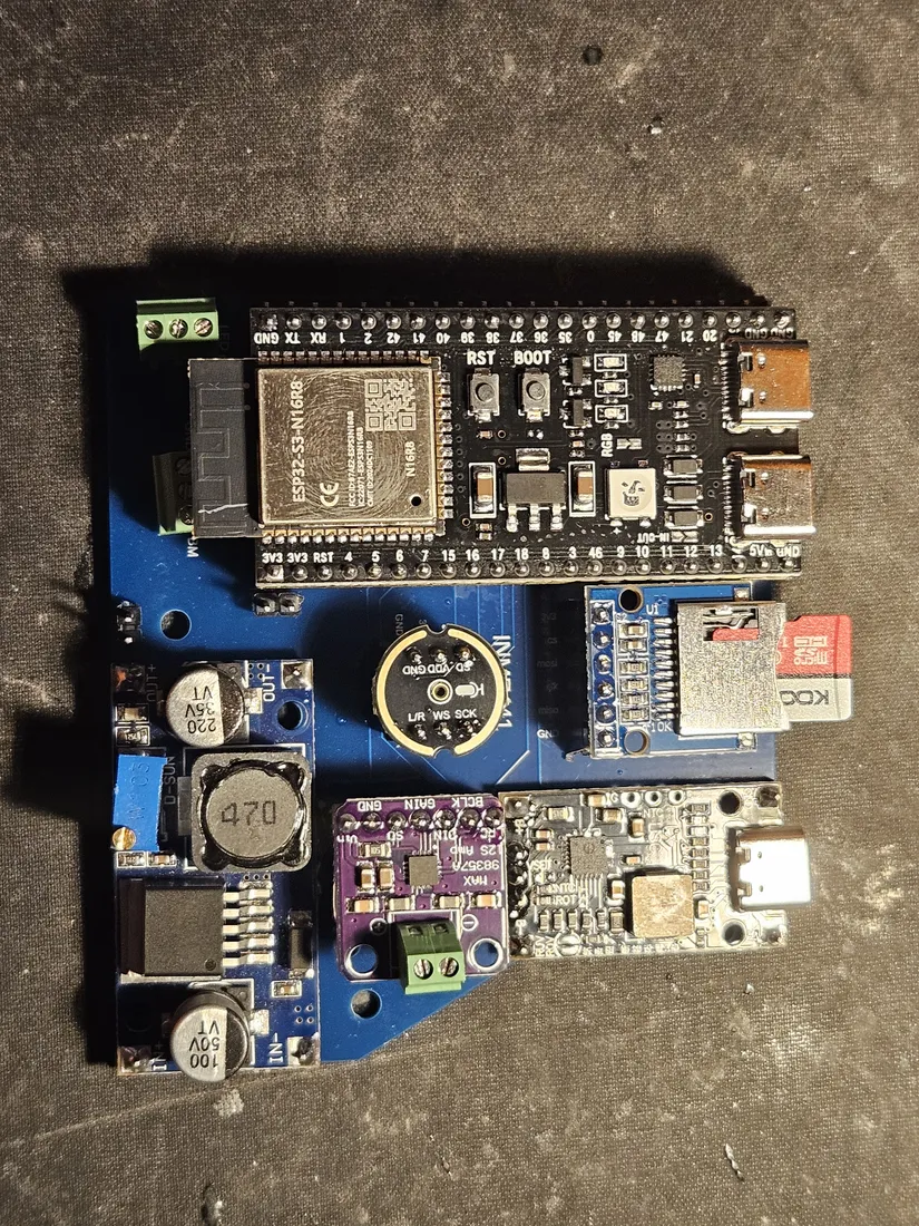
Confirm the stack matches Wiring. Top-down, every module from the pinout tables is present and seated: the ESP32-S3-N16R8 DevKit up top (both USB-C ports, RST and BOOT buttons clear), the DC-DC buck with its 220 35V and 100 50V electrolytics, 470 inductor, and blue output trimpot, the purple MAX98357A amp beside the INMP441 mic and the buzzer, the microSD module with a card fully home, and the BMS USB-C board. Check the microSD card is seated flush, not proud - a card that stands off the socket is the cardType=0 trap. Green screw terminals carry the pack and 5 V leads; verify each is clamped on stripped copper, not on insulation. Keep the 2S BMS between the cells and everything else, and never charge the pack outside the BMS - charge only through its USB-C port. Use brand-name cells from a reputable vendor (counterfeits are common); see the 2S Li-ion safety note in the BOM.
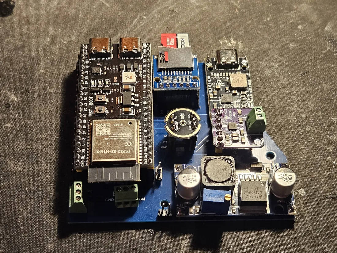
Check the vertical stack from the side. The tall parts - the DevKit module can, the two DC-DC electrolytics, the amp and mic breakouts - all clear each other with no board bowing and no header touching a neighbor's pads. The blue PCB seats down onto the printed standoff frame with an even gap all around; no component is crushed against the frame. Reconfirm every ground is common here (Power architecture): cells, BMS, DC-DC, ESP32, and every module share one GND. A missing common ground reads as flaky peripherals, not a dead board.
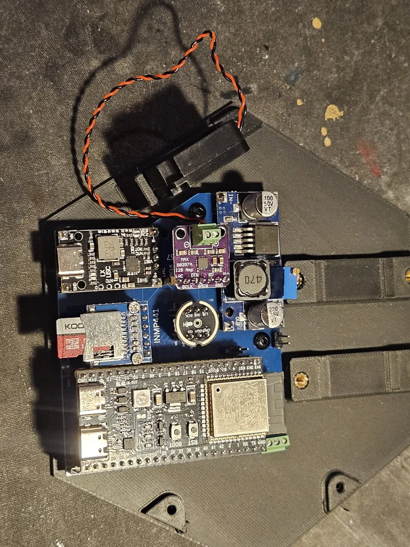
Seat the PCB into the printed bottom case. Lower the assembly so the board mounting holes line up over the case's screw posts and brass heat-set inserts. It should drop in without forcing - if it fights, find the tall part or lead that is catching before pressing harder. Drive the case screws into the brass inserts snug, not hard; the insert strips before the plastic complains, so stop at first resistance rather than chasing a number.
Route every lead so nothing is pinched. Before the screws go tight, sweep all wiring - the twisted red/black lead pair and any module still to be secured - clear of the board edges, screw posts, and the case wall so nothing is trapped or crushed when the case closes. Pinched insulation is a short waiting to happen. Give the pack and 5 V-bus leads a gentle tug to confirm the screw terminals hold.
Set the buck to 5 V before the pack feeds the stack. The DC-DC output is adjustable at the blue trimpot, so never trust it blind. With the pack connected to the buck input but the 5 V lead still off the board, meter the buck output and confirm it reads 5 V before you land it on the bus. A buck left high pushes past 5 V into every board on the 5 V bus and destroys them.
One last power-on before the lid. With the stack in the case but still openable, power up and confirm the device boots and the self-test still passes in its installed position - a fault that only appears after seating is almost always a pinched lead or a ground gone open. Keep a hand near the modules for the first minute: a warm or hot module or SD card is an electrical fault - kill power immediately and find the short before going further (hot-card safety check). Only then install the production firmware (Assembly order step 7) and close the case.
The firmware caps LED-ring brightness at 60%; leave it there. Raising it pushes ring current and heat past what the 5 V bus and this enclosure are sized for.
Fit the touch TFT
This is the 2.8" ILI9341 240×320 panel with the XPT2046 resistive touch controller. It carries the display, the touch layer, and a microSD socket on one red module. The touch layer is the only input (see The three on-module solder bridges (do this first) and the wiring table).
Do the bridges first. Before the module goes anywhere near the enclosure, the three on-module touch-to-display bridges must already be soldered and continuity-checked with power disconnected. That is not part of this step - it is the prerequisite for it. If you have not done it, stop and complete The three on-module solder bridges (do this first) now. A missing bridge is the number-one build fault and produces a blank display or dead touch with no error anywhere.
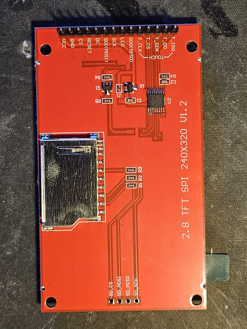
Identify the pads before wiring. Work from the back of the module. The long header along the top carries the display and power pins - VCC, GND, CS, RESET, DC, SDI(MOSI), SCK, LED, SDO(MISO) - and the touch pins T_CLK, T_CS, T_DIN, T_DO, T_IRQ. The silk reads 2.8 TFT SPI 240×320 V1.2; confirm yours matches. The microSD socket and its own SD_CS / SD_MOSI / SD_MISO / SD_SCK pads sit lower on the board - those are the separate SPI2 bus and are not part of this panel's wiring. Land each wire per the TFT + touch (SPI3) table. Leave T_IRQ unconnected.
Seat the module in the lid. Mount the panel face-out in the enclosure lid so the glass sits centered inside the WS2812B ring, as shown. Route the display and touch harness back to the ESP32-S3 carrier in the base, keeping the bundle clear of the ring so the lid can close. Dress the wires so nothing is pinched at the hinge. The base carries only the DevKit and the shared peripherals (mic, amp, microSD, power section), and the panel is the sole input.
Check before you close it up.
- Every ground is common - the panel
GNDties back to the same node as the cells, BMS, DC-DC, ESP32, and every other module. - The panel
VCCis on 3.3 V, not the 5 V bus. - Run the bring-up sketch (
pio run -e tftbringup -t upload) and confirm color bars, the backlight fade, and raw touch before installing the production firmware. Uncalibrated touch looks identical to broken touch, so calibrate (Touch calibration) before concluding anything is miswired. - If the panel or the SD card ever runs warm or hot, that is an electrical fault: power off first, then investigate (hot-card safety check). A shorted SD socket can brown out or damage the display even though the two buses are separate.
The backlight is a continuous draw whenever the screen is lit. It sits on a PWM pin and the firmware blanks it when idle. The firmware caps LED ring brightness at 60%; do not raise it.
Assembly order
The photo-by-photo build is the Assembly walk-through above; the same shots gathered on one page are the build photos.
- Solder the three touch-to-display bridges on the module and continuity-check them (section above). Doing this before any board wiring makes the check unambiguous.
- Bench-check the bare DevKit. Flash it over the UART USB-C port - on a factory-fresh board the native USB port has no path into download mode, so getting this wrong looks like a dead board. See First flash of a fresh board.
- Wire the TFT module per the table above, then run the standalone
bring-up sketch - it exercises the panel, colors, backlight, and raw touch
without the full firmware:
pio run -e tftbringup -t upload
- Wire the remaining 3.3 V peripherals on USB power - microSD, mic, amp.
- Build the power section separately: cells into the 2S BMS, BMS output into the DC-DC. Verify a clean 5 V at the DC-DC output with a meter before connecting anything.
- Connect the 5 V bus: LED ring +5V and the ESP32 VIN. Confirm every ground is common.
- Add the battery-sense divider if you want a battery gauge.
- Install the production firmware with the guarded installer:
The installer storespython3 tools/setup_device.py
scrModel=tftso the board binds its display and touch drivers on the first boot. - Calibrate the touch panel. Every resistive panel reads differently, so
the raw-count-to-pixel mapping is measured per unit - until it is set,
taps land somewhere else and touch looks broken. Run the wizard:
Full detail: Touch calibration.python3 tools/tcal_wizard.py --port /dev/cu.usbserial-XXXX
Known traps
- The three bridges are the number-one build fault. A missing bridge produces a blank display or dead touch with no error anywhere - see the continuity check above.
- Reachable GPIOs are nearly all consumed. Only the J3 header is reachable
on the carrier, GPIO 35/36/37 (octal PSRAM) sit in the middle of it, and the
longest usable contiguous run is seven pins (
1, 2, 42, 41, 40, 39, 38) - all consumed by the panel. The documented free spares are on J1, which the carrier does not break out. GPIO 47 is the only genuinely free reachable pin on this variant. - The backlight is a continuous draw. Plan for it in battery estimates; the firmware blanks it when idle rather than drawing a screensaver, because on a TFT showing nothing is cheaper than showing anything.
- The touch controller is slow. The XPT2046 tops out near 2 MHz against the panel's 40 MHz, so each device gets its own SPI transaction settings. Getting this wrong does not fail loudly - it returns plausible-looking garbage coordinates.
- Uncalibrated touch is indistinguishable from broken touch. Calibrate before concluding anything is miswired (Touch calibration).
- The SD card must be FAT32, not exFAT. Cards over 32 GB ship
exFAT-formatted by default and mount as
cardType!=0, ok=false. Reformat as FAT32 ("MS-DOS (FAT)" on macOS) before first use. - A cold SD ground joint reads as
cardType=0- the card looks absent, not faulty. Check continuity from the SD module's GND to system GND before suspecting the card. - A warm or hot SD card is an electrical fault. Disconnect power immediately - see the hot-card safety check. An SD power fault can brown out or damage the display even though the buses are separate.
- Never route anything to GPIO 33–37 (octal PSRAM on the N16R8), nor to 0/45/46 (strapping), 19/20 (USB), 43/44 (UART), 26–32 (flash).
- If the panel ever goes blank white, read the white-screen investigation before re-measuring anything - the field cause was traced to the device's own SoftAP radio disturbing a jumper-wired panel, the firmware now avoids it, and a watchdog bounds any residual symptom to about 5 seconds.
Battery pack
Two 18650 cells in series (2S, 6.0–8.4 V range) behind the BMS. Ground truths from the reference pack, measured on a dedicated analyzer: 3500 mAh capacity, 8.40 V full. Measured runtimes on that pack: 5.75 h at ring brightness 77/255 (608 mA average), about 23 h idle (~150 mA). The TFT backlight adds continuous draw on top of those figures whenever the screen is lit. Details in Measured battery reality.
Note that the ADC under-reads a full pack - after assembly, charge fully and
run BATTCAL (console) so 100 % reads as 100 %. See
Battery voltage sampling.
Enclosure and CAD
A 3D-printable enclosure for this build is published:
hardware/fab/nimbus_classic_case.stl
(GitHub renders it in a 3D viewer). Print in PLA or PETG; the main body needs no
supports on most printers. The
hardware/fab/ folder
also holds the PCB manufacturing outputs (Gerbers, ODB++) and
how to order the board.